K-MAP Implemented with a MUX
Question:
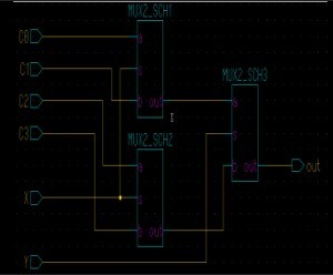
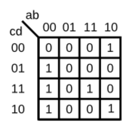
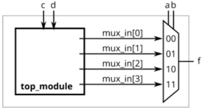
For the following Karnaugh map, give the circuit implementation using one 4-to-1 multiplexer and as many 2-to-1 multiplexers as required, but using as few as possible. You are not allowed to use any other logic gate, and you must use a and b as the multiplexer selector inputs, as shown on the 4-to-1 multiplexer below.
Solution:
To implement the given K-map function using only multiplexers, follow these structured steps:
Step 1: Implement a 4-to-1 Multiplexer
The 4-to-1 multiplexer is already implemented in Weekly Blog 1. Before proceeding, ensure that it functions correctly by checking that:
When
a = 0b = 0→mux_in[0]is selectedWhen
a = 0b = 1→mux_in[1]is selectedWhen
a = 1b = 0→mux_in[2]is selectedWhen
a = 1b = 1→mux_in[3]is selected
If you haven't implemented it yet, refer to Weekly Blog 1 for the Verilog code of the 4-to-1 multiplexer.
Step 2: Determine Inputs for 4-to-1 MUX (I0, I1, I2, I3) using K-map
When a = 0, b = 0 : mux_in[0] = c+d
When a = 0, b = 0 : mux_in[1] = 0
When a = 0, b = 0 : mux_in[2] = ~d
When a = 0, b = 0 : mux_in[3] = c
Step 3: Verilog Code for Implementing the Function using MUX
Step 4: Verilog Testbench for the MUX-Based Implementation
Now that we have designed our circuit using multiplexers, we need to verify its correctness using a testbench. The testbench will simulate all possible input combinations and ensure the output matches the expected values derived from the K-map.
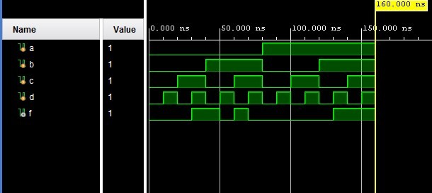
Step 5: View the Waveform (Timing Diagram)
After running the testbench:
Conclusion
In this exercise, we successfully designed and verified a multiplexer-based circuit implementation using one 4-to-1 MUX and multiple 2-to-1 MUXes. The key takeaways from this implementation are:
✅ Understanding Karnaugh Maps (K-maps): We derived the Boolean function from the K-map and implemented it using multiplexers without additional logic gates.
✅ Efficient Multiplexer Usage: Instead of using traditional logic gates, we demonstrated how MUXes alone can implement combinational logic efficiently.
✅ Verilog Implementation & Simulation: We wrote the Verilog code for both the design and testbench and simulated the circuit to verify its correctness.
✅ Timing Diagram Verification: The output f matched the expected truth table values for all 16 input combinations, confirming the correctness of our design.