Design and Implementation of a CMOS Inverter using Sky130 Technology: From Schematic to Layout
Overview
This project demonstrates the complete custom VLSI design flow of a CMOS inverter using the open-source Sky130 technology. Starting from schematic design in Xschem, we simulate the inverter’s electrical behavior with ngspice, then implement and verify its physical layout in Magic. This end-to-end process highlights fundamental concepts in VLSI design and serves as a building block for more complex digital circuits.
Introduction
In this project, we explore the full custom design flow of a CMOS inverter using the Skywater 130nm process (Sky130). We begin by designing the inverter schematic in Xschem, performing detailed electrical simulations in ngspice to analyze its behavior, and proceeding to create a layout in Magic. Finally, we verify the design through Design Rule Check (DRC) and Layout Versus Schematic (LVS) checks, ensuring the physical layout matches the intended circuit functionality.
This project not only illustrates the theoretical principles of inverter operation but also provides practical hands-on experience with industry-standard EDA tools and open-source silicon processes. It serves as a solid foundation for anyone interested in integrated circuit (IC) design and custom VLSI workflows.
Schematic Design
The first step in designing a CMOS inverter is creating its schematic at the transistor level. A CMOS inverter consists of a PMOS transistor connected between VDD and the output, and an NMOS transistor connected between the output and ground. Both gates are tied together to form the input signal.
In this project, I designed the inverter schematic using Xschem, an open-source schematic editor compatible with the Sky130 PDK.
Design details:
PMOS transistor:
Source connected to VDD
Drain connected to the inverter output
NMOS transistor:
Source connected to GND
Drain connected to the inverter output
Gates of both transistors connected to the inverter input
W/L sizing chosen based on desired switching threshold and drive strength
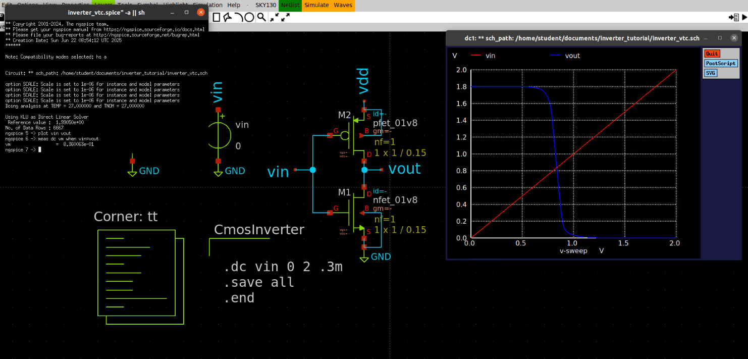
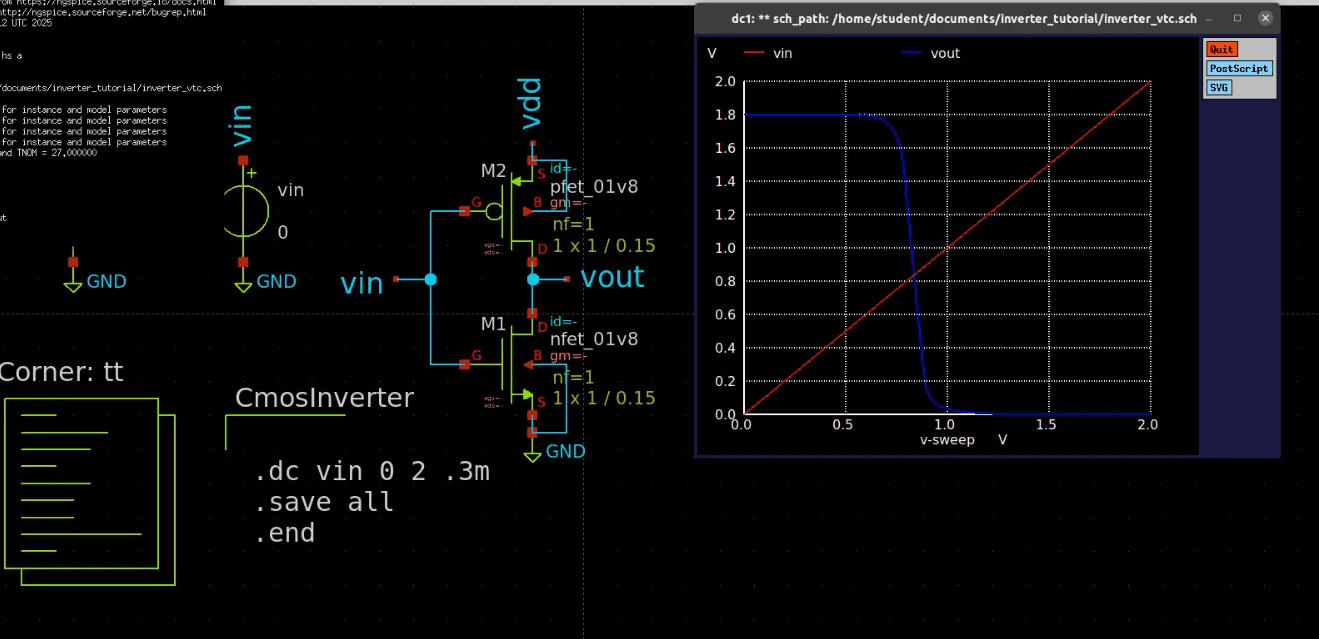
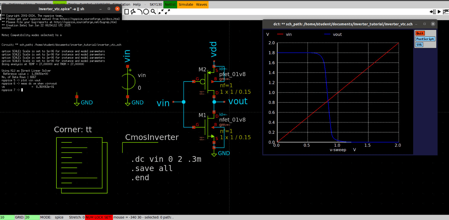
Simulation Results – DC Sweep Analysis
To analyze the static behavior of the CMOS inverter, I performed a DC sweep simulation in ngspice. The goal of a DC sweep is to determine how the inverter’s output voltage (Vout) varies as the input voltage (Vin) transitions from 0 V to the supply voltage (VDD). This helps identify the inverter’s switching threshold, also known as the trip point (Q-point), which is the input voltage at which the output voltage transitions sharply from high to low.
Initial Simulation – Equal PMOS and NMOS Widths
Initially, I designed the inverter with the same width for both PMOS and NMOS transistors:
PMOS width (Wp) = NMOS width (Wn)
In this configuration, both transistors have equal drive strength under ideal conditions.
However, due to inherent differences in mobility between electrons (NMOS) and holes (PMOS), an inverter with equal transistor sizes often does not switch exactly at half of VDD.
Modified Simulation – Wider PMOS
To shift the inverter’s switching threshold closer to the midpoint of VDD, I increased the PMOS transistor width by a factor of 2:
New Wp = 2 × Wn
Increasing the PMOS width compensates for the lower mobility of holes compared to electrons, thus balancing the pull-up and pull-down strengths of the inverter.
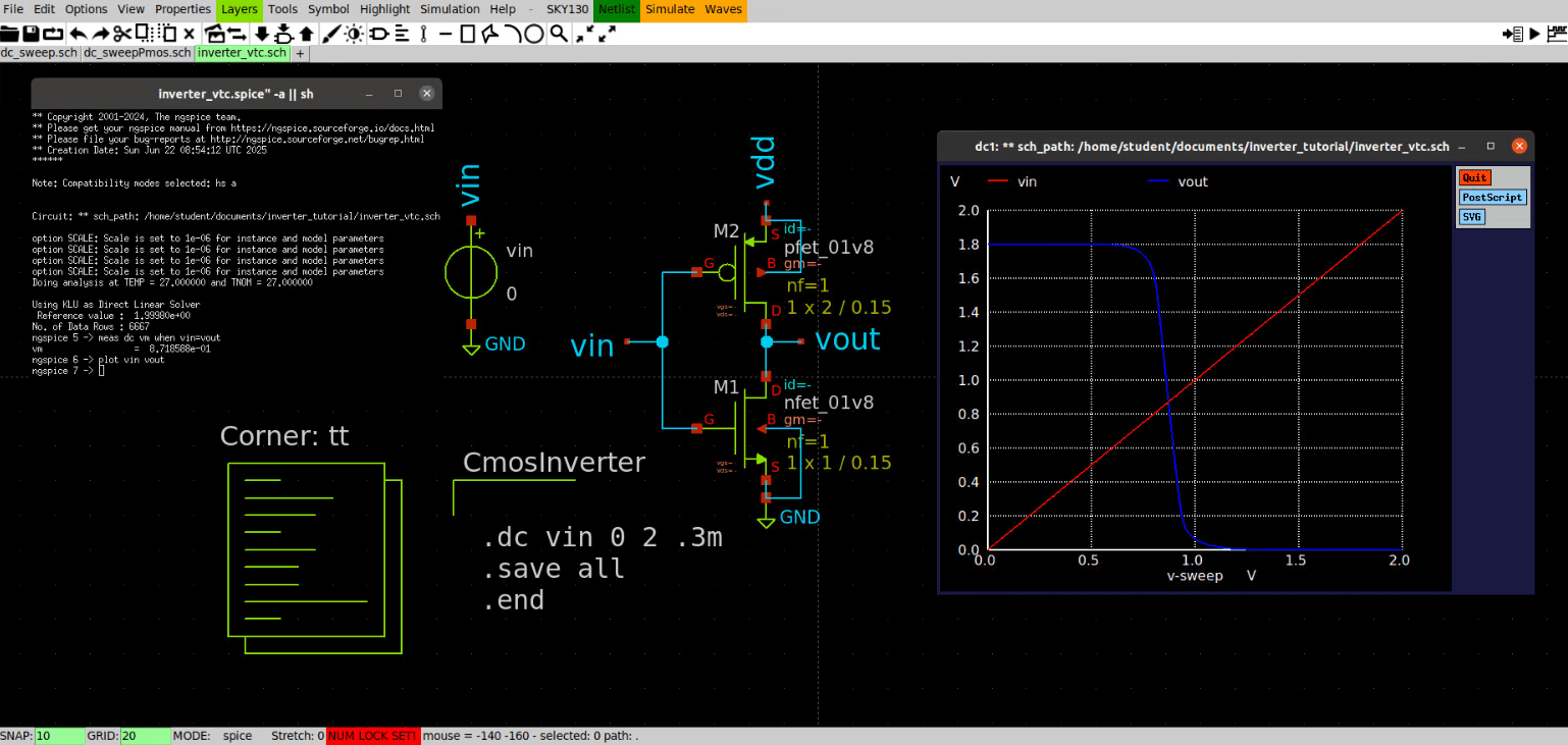
Result:
After increasing the PMOS width, the trip point moved to approximately 8.79 units.
This shift indicates:
The inverter now switches states at a higher Vin than before, closer to half of VDD.
The inverter becomes more balanced in terms of rising and falling transition strengths, improving noise margins and ensuring symmetrical switching behavior.
Observations
The shift from 8.31 → 8.79 demonstrates how transistor sizing directly impacts the inverter’s DC characteristics.
Proper transistor sizing is crucial for:
Symmetrical voltage transfer characteristics
Optimized noise margins
Balanced propagation delays
Bottom Line
✅ Doubling your PMOS width improved your inverter’s balance.
✅ Your inverter now has excellent noise margins (~0.8–0.9 V), perfect for robust digital logic.
Layout Design in Magic
After completing the schematic design and simulations, the next step was to translate the inverter circuit into a physical layout using Magic VLSI, an open-source layout editor compatible with the Sky130 process. The layout defines how transistors, metal layers, and interconnections are physically realized on silicon.
For this inverter layout:
The PMOS transistor was placed at the top, connected between VDD and the output.
The NMOS transistor was placed at the bottom, connected between the output and GND.
The gates of both transistors were tied together to form the inverter input.
The inverter output (VOUT) was routed using Metal1.
Contacts and vias were added where necessary to connect diffusion regions to metal layers.
Power rails (VDD and GND) were implemented using Metal1 for easy access and future integration into larger circuits.
The layout was carefully drawn to follow the Sky130 design rules, ensuring minimum spacing, enclosure, and width requirements for all layers.
Layout Dimensions
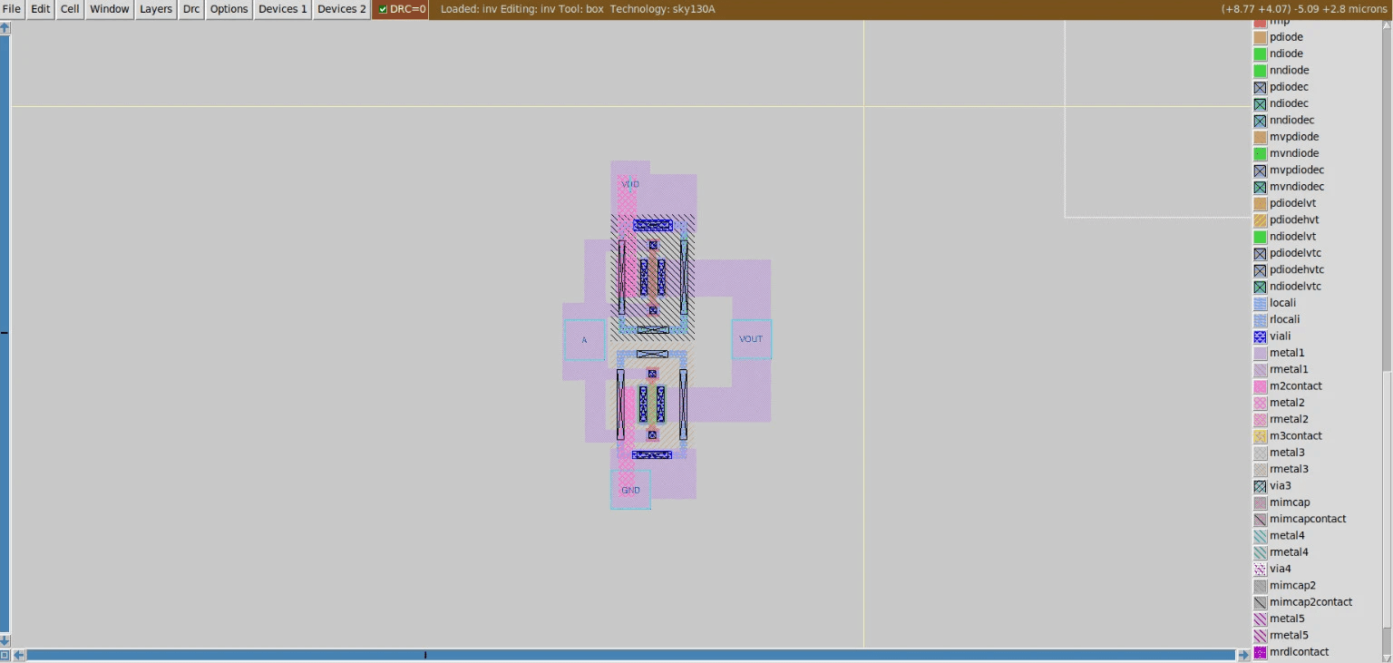
The inverter layout occupies an area of approximately 8.77 μm × 4.07 μm
This compact size makes it suitable for inclusion in standard cell libraries.
Design Rule Check (DRC)
Once the layout was completed, I performed a Design Rule Check (DRC) in Magic. The DRC verifies that all polygons, contacts, and layers comply with the manufacturing constraints defined in the Sky130 technology file.
Why DRC is Important
Passing DRC is a critical step in VLSI design because:
Violating design rules can result in fabrication defects.
Ensures that transistors and interconnections will work correctly once fabricated.
Avoids costly tape-out failures.
Next Steps
After completing the inverter layout and verifying it with DRC, the following steps complete the full custom design flow:
LVS Check: Ensure the layout’s netlist matches the original schematic, confirming the physical design implements the intended circuit.
Parasitic Extraction (Optional): Extract RC parasitics from the layout to simulate real-world effects like additional delay or capacitance.
Re-Simulation: Run simulations with parasitic data to analyze the inverter’s performance accurately.
Conclusion
This project successfully demonstrated the complete custom design flow of a CMOS inverter using the Sky130 open-source process. Starting from schematic design in Xschem, I analyzed the inverter’s electrical behavior through DC and transient simulations in ngspice, explored the impact of transistor sizing on switching thresholds and noise margins, and created a physical layout in Magic VLSI.
Achieving zero DRC errors confirmed the layout’s compliance with fabrication rules, making it ready for further steps like LVS verification and parasitic extraction. Through this project, I gained practical experience in both the circuit-level design and the physical layout process, reinforcing essential concepts in VLSI design.